Optimizing Data Movement with Shared Data Memories#
Goals#
Introduction to the data memories of the compute tiles.
Explore dataflow between neighboring compute tiles via task level parallelism.
Understand how ping-pong buffering is implemented with data memory banks to optimize dataflow between neighboring tiles.
Learn how to achieve overlapped compute and data movement.
References#
Introduction#
In the previous sessions we used the color threshold example to explore data movement and data parallelism. In this section we will focus on dataflow between neighboring compute tiles using their local data memories to achieve task level parallelism using an edge detection example.
Dataflow and Task Level Parallelism#
The edge detection dataflow graph is shown below.
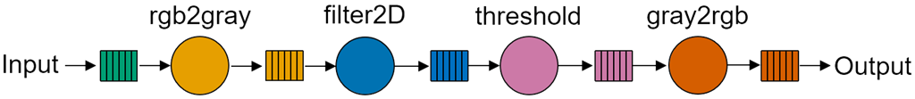
There are four kernels in this application:
rgb2graytransforms the RGB color image into grayscalefilter2Dis a 2D filter that implements edge detection using a Sobel operatorthresholdsets a noise floor threshold for the applicationgra2rgbconverts the stream back to RGB format for display, although the video stream will be grayscale
Each (compute) kernel can start operating on the input buffer as soon as it receives sufficient data from the previous kernel. In the case of this algorithm, a 3x3 2D filter is used where each kernel needs two full lines of the image plus the next three pixels for each calculation. The dataflow graph shows a sequential chain of operations with only data dependencies between sequential kernels. i.e., the last kernel gray2rgb depends on data from threshold, threshold depends on filter2D and so on.
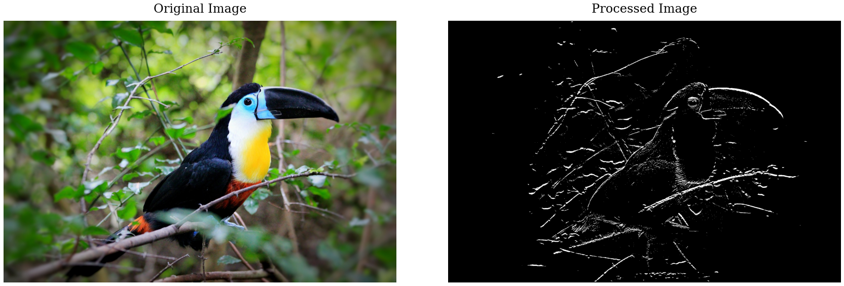
In the image below you can see the result of the edge detection.
Implementation#
This example could be mapped and run on the NPU in different ways. All four kernels of this application could be run sequentially on a single compute tile. The rgb2gray kernel receives RGB data, converts it to grayscale, and writes the grayscale data to memory. The filter2d kernel could then run in the same compute tile, read the grayscale data, processes it, and write its results to memory, and so on. The performance of this application with all four kernels running on a single tile would be low relative to the available compute resources in the array.
Alternatively, each of the four kernels could be mapped to a compute tile in a single column and carry out their processing on the video stream concurrently. This is known as task level parallelism - distributing tasks across different processors in a multi-core system. It would take some time for the initial data to flow through the kernels and produce the first results, but once each kernel has data, using four compute tiles should increase the throughput of the system. This should give some immediate speed-up to the whole application as we are now using 4x the number of compute resources. However, the performance of the application would now be determined by the data movement between the kernels and if the system can supply data to the pipeline at a fast enough rate to benefit from the available compute resources.
Run the Edge Detection Example#
Run the following cell to start the example:
from npu.lib import EdgeDetectVideoProcessing

app = EdgeDetectVideoProcessing()
app.start()
NPU Resource Utilization#
In all, the application uses:
1 interface tile
2 data movers
1 for stream input and 1 for stream output
4 compute tiles
1 for each of the kernels
5 memory buffers
2 memory buffers placed in the data memory at the top
1 memory buffer in the remaining compute tiles
2 data movers
1 for stream input at the compute tile in the top
1 for stream output at the compute tile in the bottom
Visualize the Application#
You can visualize an animation of the application running on the NPU by running:
app.display()
You can visualize the output in the animation below.

Data Memory and Memory Banks#
Compute tile data memory#
We saw in previous sections that the data memory in the compute tiles is 64KB in size and arranged into 8 banks of 8KB each. There are four memory ports to the data memory, north, south, east and west represented in blue in the diagram below. The memory port on the west is connected to the local AI Engine.
Each of the banks can be accessed independently through these ports, although only one port can access a bank at a time. Different banks can be accessed simultaneously.
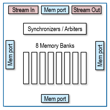
The data memory also has synchronizers and arbiters that will control access to the memory banks.
The data memory can also be accessed via stream interfaces from non-neighboring tiles. This tile can send data to non-neighboring tiles via the same interfaces. The stream interfaces are the only way to move data from interface or memory tiles into and out of compute tiles. They are used in every Ryzen AI application. As the stream interfaces have been discussed in previous sections, they will not be discussed in this example.
Nearest-Neighbor Data Memory Sharing#
Accessing multiple memories from a single AI Engine processor#
Each AI Engine processor has the capability to access a total of four distinct data memories. The first one is its own local data memory located within its own tile, memory to the east of the AI Engine. Additionally, there are three other data memories situated in the adjacent compute tiles, namely to the north, south, and west.

The AI Engine processor can access data memories up to four times the size of its own local data memory, which effectively means it can access a 256KB memory pool. Furthermore, multiple AI Engines can collaborate by sharing access to the same memory, enhancing the overall performance of applications running on the NPU. This shared memory arrangement allows data to be accessed directly between kernels executing on different AI Engines. For instance, one kernel running on a processor can write results to a data memory, whether it is the one in its own tile or a neighboring tile. Subsequently, another kernel executing on a neighboring tile can retrieve these results from the same data memory. This boosts application performance while minimizing data transfers, which, in turn, reduces efficiency and lowers power consumption.
It is important to note that the local data memory is distinct from the instruction memory for each AI Engine processor. Each AI Engine has its own 16KB instruction memory which is not shared among processors.
Accessing the same memory from different AI Engine processors#
Another perspective on the data memories is that a memory within a single tile can be accessed by up to four AI Engine processors: the AI Engine in the same tile and up to three AI Engines in adjacent tiles situated to the north, south, and east, as indicated in the diagram:

It is important to clarify that tiles positioned at the edges of the NPU array can have fewer memory connections as they may lack neighbors in some directions. For instance, the tiles in the top row do not have a neighboring tile to the north. Consequently, these top-row tiles do not have a memory interface to the north and cannot share their memory data in that direction.
Most AI Engines can access three data memories in their neighboring compute tiles to the north, south and west, as shown above.
Here is a summary how many data memories each type of cell can access:
Tiles that can access 2 local data memories#
The compute tile in the top left corner of the NPU array can access 1 local data memory and 1 more in the neighboring tile to the south.
The compute tile in the bottom left corner of the NPU array can access 1 local data memory and 1 more in the neighboring tile to the north.
There are \(2\) tiles that can access 2 local data memories.
These tiles are colored pink in the diagram below.
Tiles that can access 3 local data memories#
The other compute tiles along the top row of the NPU array can access 1 local data memory and 2 more in their south and west neighbors.
The other compute tiles along the bottom row of the NPU array can access 1 local data memory and 2 more in their north and west neighbors.
The remaining compute tiles in the leftmost column of the NPU array can access 1 local data memory and 2 more in their north and south neighbors.
For an \(4 \times 5\) NPU array, there are \(10\) tiles that can access 3 local data memories.
These tiles are colored green in the diagram below.
Tiles that can access 4 local data memories#
Compute tiles in the middle of the array, and the remaining compute tiles in the middle of the last column can access 1 local data memory and 3 more in their north, south and west neighbors.
For an \(4 \times 5\) NPU array, there are \(8\) tiles that can access 4 local data memories.
These tiles are colored blue in the diagram below.

This architecture helps minimizing data movement as data can be read in place from one compute tile and processed in another. This also helps data reuse as data does not have to be transferred to the memory of every compute tile that needs this data. The compute tiles contain synchronizers and locks to control access to memory buffers between different compute tiles.
While two compute tiles cannot access the same memory location simultaneously, two compute tiles can access different banks in the same data memory. Applications can take advantage of this feature by synchronizing the reading and writing of data between kernels across different banks. This is called ping-pong buffering.
Ping-pong Buffering#
Ping-pong buffering is a computing technique used to efficiently transfer data between two processes. One process generates data and writes it into a buffer. The other process consumes data and reads it from the buffer.
Basic operation of ping-pong buffers#
The operation of ping-pong buffers can be understood as follows: as one buffer is actively written to, it gradually fills up with data. Simultaneously, the other buffer is being read from, causing it to empty. When the write buffer becomes full at the same time the read buffer becomes empty, they switch roles. The formerly empty buffer becomes the new write buffer and starts to accumulate data, while the previously full buffer becomes the read buffer and begins to be emptied.
This mechanism allows both processes to access the buffer concurrently, with one writing while the other reads. Ping-pong buffering effectively minimizes latency and enhances data throughput, making it particularly useful in real-time applications.
Ping-pong buffer example:
To understand this concept, let us assume that we have kernel A and B. Kernel A is the producer and writes data that is read by kernel B, the consumer.
A writes to the ‘ping’ buffer, filling it. B reads from the ‘pong’ buffer, emptying it. Once A fills its current ‘ping’ buffer, while at the same time B empties its ‘pong’ buffer, the two kernels switch the buffers they are operating on and continue.
If the buffers are placed in different banks of memory, both buffers can be accessed concurrently.
Consider the kernels in the dataflow graph for the edge detection example and the following sequence:
The pink kernel representing the first compute node will take control of one bank of a data memory by locking it. This means it has exclusive access to this bank. It can then write its output data to this bank.
Once the first kernel fills the bank (or writes sufficient data for the second kernel to start computing), the first kernel releases its bank.
As the first kernel releases the first bank, the second compute node can now take control of this bank and start reading the data it needs.
The first kernel switches to the next available bank, locks it, and continues writing its data to the new bank until it fills it
Once the second kernel has consumed the data from the first bank, it releases it, and switches reading data to the next bank, which the first kernel has just finished filling.
The first kernel can reuse the initial bank or use the next available bank and the process continues.
This is the essence of ping-pong buffering. Rather than a sequential set of steps, both kernels operate concurrently.
You can see an animation illustrating these steps and ping-pong buffers:
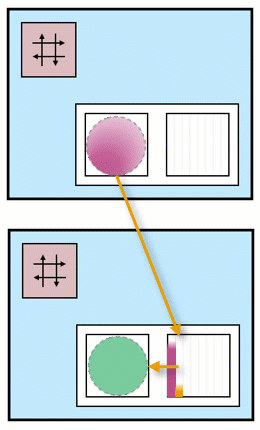
In the top compute tile, there is a pink kernel that generates data. This data is stored in two separate buffers, one pink and one orange. These buffers are located in different banks within the data memory.
In the second compute tile, there is a green kernel that consumes data from these two buffers.
As one of the buffers is being filled by the pink kernel, the other one is simultaneously being emptied by the green kernel. This ensures a continuous flow of data between the two kernels, with one producing data while the other consumes it.
In this example, we are using the data memory in the second compute tile. It is important to note that both tiles have access to each other’s data memory. This means that the memory buffers we are using in the second tile could also be located in the data memory of the top tile.
Overlapping Compute and Data movement#
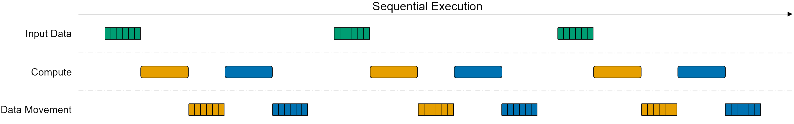
Assuming the data is generated by one tile and consumed by the other at the same rate, by using ping pong buffers data can be transferred and processed continuously by both compute tiles. The alternative would be for the first tile to transfer data, wait for the next tile to process it before computing and sending new data. You can see the effect of a sequential execution in the image below. The blue kernel cannot start processing until the data movement of the orange kernel completes.
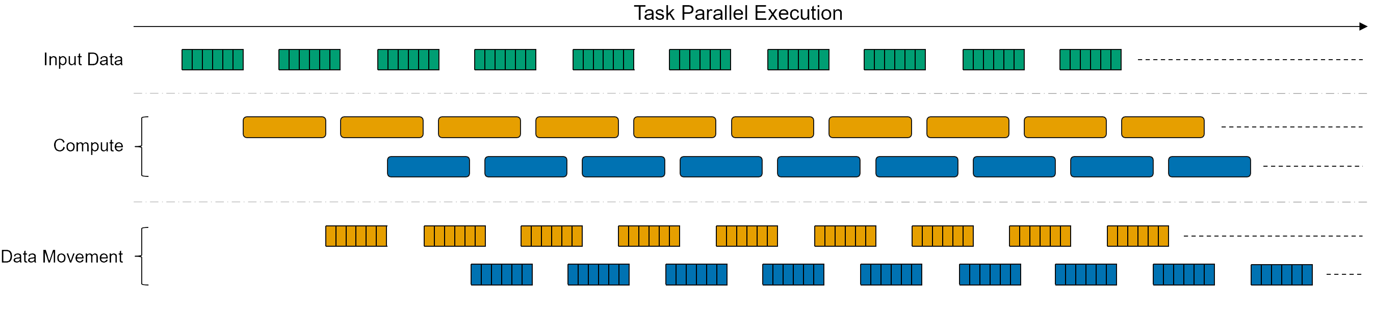
Overlapping compute and data movement increases the utilization of the processors in the compute tiles, significantly improving the performance of the application. The image below shows a task parallel execution, where each kernel runs independently. The ping pong buffering allows to overlap the data transfer and computation as shown in the image. The availability of data still triggers the execution of the compute kernels, however in this scenario both of them run simultaneously. This concept can be extrapolated to a data flow graph with more kernels.
Note that if the first kernel is mapped to the compute tile at the top of a column, and the second kernel to the tile below it, ping-pong buffer can be placed in the data memory for either tile. The flexibility of this architecture is a big advantage for more complicated designs where resources may be constrained.
In this simple example we assumed two banks were used for ping-pong buffering. The number of buffers used will depend on factors including the size of the data that needs to be transferred between tiles, the rates data is generated and consumed in each tile, and any other data dependencies - for example a kernel may require data from more than one source. An application may use multiple memory banks to overlap data movement and compute.
The compiler will manage the allocation of memories and banks and manage the memory locks and synchronization between kernels.
Task Level Parallelism#
The edge detection example in this section uses task level parallelism. Each of the kernels is mapped to a different compute tile and is executed independently driven by the availability of input data for each kernel.
Task level parallelism is another way of increasing the performance of your design in a multi-core dataflow architecture.
Next Steps#
In the next notebook we will explore efficient data movement using shared data memories and streaming interfaces.